
2 Nm Film Tweaks Just Gave Metals a New Control Knob
2 Nm Film Tweaks Just Gave Metals a New Control Knob https://torontostarts.com/silicon-scoop/ Flowgrammer.ca -> https://flowgrammer.ca/ AI News and Resources -> https://flowgrammers.ca OpenClaw Toronto -> https://openclawto.com/ Stop Doing Work Your Software Should Do Automate admin, handoffs, follow-ups, and reporting so your team gets hours back every week—without hiring. Book an automation consult https://flowgrammer.ca Startup Investor Drinks Toronto - https://startupdrinksto.com/ Toronto’s Startup Community - https://torontostarts.com/ Silicon Scoop Silicon Scoop Podcast - https://torontostarts.com/silicon-scoop/ Apple: https://podcasts.apple.com/us/podcast/silicon-scoop/id1758711826 Spotify: https://open.spotify.com/show/5bAzF0MwV6TtLhJAhvHayI YouTube: https://www.youtube.com/playlist?list=PLj4v-RoA7A-gT62vrEYqh1zCv-0Hj-o5J Startup Talk Startup Talk Podcast -> https://torontostarts.com/startup-talk-toronto-startup-podcast/ Apple -> https://podcasts.apple.com/us/podcast/startup-talk/id1763804003 Spotify -> https://open.spotify.com/show/1siJMILILidHAiAsrX2VBU YouTube: https://youtube.com/playlist?list=PLj4v-RoA7A-jxV5FHs5e61oIsuvUJYmT_&si=LYegRe5GYLKNQ7xL
With Craig Major and Jon Irwin
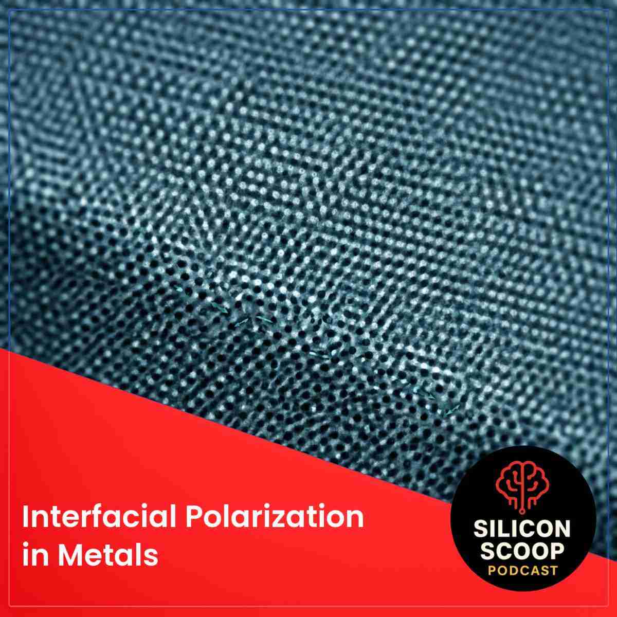
Interfacial Polarization in Metals: How Scientists Can Now Control Metal Behavior One Atom at a Time
Estimated reading time: 10 minutes
Key Takeaways
- Interfacial polarization in metals can be stabilized through careful interface design, allowing polarization effects inside a metallic system.
- The work function of RuO₂ can be tuned by more than 1 electron volt by changing film thickness by just 2–3 nanometers.
- A critical transition occurs at approximately 4 nanometers, where RuO₂ shifts from fully strained to relaxed, driving major electronic changes.
- Scientists confirmed the effect using multislice electron ptychography and Kelvin probe force microscopy (KPFM).
- The discovery points toward advances in electronics, quantum devices, and catalysis, and has implications for semiconductor policy and export controls.
Table of contents
- Interfacial Polarization in Metals: How Scientists Can Now Control Metal Behavior One Atom at a Time
- Introduction: A Discovery That Changes How We Think About Metals
- What Is Interfacial Polarization — and Why Does It Matter in Metals?
- RuO₂/TiO₂ Heterostructures: The Experiment That Made It Real
- How Scientists Saw It: Visualizing Atomic Displacements
- Why Work Function Tuning Changes the Game for Electronics
- Quantum and Catalytic Devices: Two More Frontiers
- What This Means for Semiconductor Policy and Export Controls
- The Bigger Picture: From a Fixed Contact to a Tunable Design Element
- FAQ: 10 Questions About Interfacial Polarization in Metals
Introduction: A Discovery That Changes How We Think About Metals
Interfacial polarization in metals was not supposed to be possible — at least not in any useful, controllable way.
For decades, scientists treated polarization as something that only happened in insulators and special materials called ferroelectrics. Metals were seen as fixed. Predictable. Not something you could “tune” like a dial.
That thinking just changed.
Researchers at the University of Minnesota Twin Cities have shown that you can shift a metal’s electronic behavior by more than 1 electron volt — simply by controlling what happens at the boundary between two materials at the atomic scale.
The study was published in Nature Communications on February 9, 2026. It focuses on a metallic material called ruthenium dioxide (RuO₂) layered on top of titanium dioxide (TiO₂). The results point toward faster electronics, smarter catalysts, and more powerful quantum devices.
This is not a small upgrade. This is a new design tool for an entire field.
What Is Interfacial Polarization — and Why Does It Matter in Metals?
Polarization Was Supposed to Stay Out of Metals
Polarization happens when electric charges shift slightly inside a material, creating a separation between positive and negative regions. This is common in insulators and ferroelectrics — materials that can hold an electric charge arrangement on their own.
Metals, on the other hand, have free-flowing electrons. Those electrons were thought to cancel out any polarization effects almost instantly.
That is why this discovery is so significant.
The University of Minnesota team showed that when you carefully design the interface — the boundary — between two materials, you can stabilize polarization inside a metallic system. The metal does not cancel it out. Instead, it holds it.
> “We often think of polarization as something that belongs to insulators or ferroelectrics — not metals,” said Professor Bharat Jalan, senior author of the study. “Our work shows that, through careful interface design, you can stabilize polarization in a metallic system and use it as a knob to tune electronic properties.”
What Is a Work Function and Why Should You Care?
The work function of a metal is the amount of energy needed to pull an electron out of that metal’s surface. It controls how well a metal connects and communicates with other materials in a device.
- A lower work function = electrons leave more easily = better electron emission and certain types of contacts
- A higher work function = electrons stay put = better for other types of contacts and catalytic reactions
In chip design and catalysis, being able to tune the work function is enormously powerful. It means you can optimize how a metal interacts with the materials around it — without swapping out the metal entirely.
Previously, this kind of tuning was mostly done using dopants (added impurities), complex gating systems, or by choosing a different metal altogether. All of those approaches add cost, complexity, and sometimes performance trade-offs.
The Minnesota team did it with thickness alone — no dopants, no extra gating systems.
Nature Communications article
EurekAlert news release
RuO₂/TiO₂ Heterostructures: The Experiment That Made It Real
Building the Stack: Epitaxial Growth on a Wafer-Compatible Platform
The research team grew ultra-thin layers of metallic ruthenium dioxide (RuO₂) on a titanium dioxide (TiO₂) substrate using a technique called hybrid molecular beam epitaxy (MBE).
This is important for two reasons:
- Epitaxial growth means the atoms of RuO₂ line up with the crystal structure of the TiO₂ below. This creates an atomically sharp, clean interface — the foundation of the whole effect.
- Hybrid MBE is wafer-compatible. This is not a one-off lab trick that can never be scaled. It is a thin-film platform that could, in principle, be integrated into real device manufacturing pipelines.
The RuO₂/TiO₂ heterostructure is a layered system — two different materials stacked with atomic precision. Heterostructures like this are already used in advanced semiconductor and quantum device research. Extending the concept to metallic oxides opens a new chapter.
The Critical Thickness: What Happens at 4 Nanometers
Here is where the physics gets fascinating.
When the RuO₂ film is very thin, it is “stretched” — forced into the crystal spacing of the TiO₂ beneath it. The atoms are under strain. This is called a fully strained state.
As the film gets thicker, the atoms start to relax back toward their natural spacing. At approximately 4 nanometers — roughly the width of a single strand of DNA — the film crosses a critical threshold. It transitions from fully strained to relaxed.
That transition is not just a structural event. It directly changes how the metal conducts electricity and how its surface interacts with the outside world.
- Below 4 nm: film is strained, atoms are packed tightly by the substrate
- At ~4 nm: critical transition point — structural and electronic shift
- Above 4 nm: film relaxes, different polarization state, different work function
The result? A work function modulation of more than 1 electron volt controlled by thickness changes of just 2–3 nanometers. That is an enormous change produced by an almost invisible physical difference.
> “This was surprising,” said Seung Gyo Jeong, first author of the study. “We expected subtle interface effects, but not such a large and controllable change in work function.”
Nature Communications article
PubMed record
How Scientists Saw It: Visualizing Atomic Displacements
Electron Ptychography: Seeing the Invisible
One of the most impressive parts of this study is not just what the team discovered — it is how they confirmed it.
To prove that polarization was actually happening at the atomic interface, the researchers used a cutting-edge imaging technique called multislice electron ptychography. This is a phase-resolved electron microscopy method that can detect incredibly small shifts in atomic positions.
Specifically, they were able to see:
- How transition metal ions (in this case, ruthenium atoms) shifted relative to surrounding oxygen octahedra
- That these polar displacements were concentrated near the RuO₂/TiO₂ interface
- That the displacements matched predictions for strain-stabilized interfacial polarization
This technique is rarely used on conductive oxide materials. The fact that it worked — and revealed such clear, measurable displacements — makes the result much more credible and detailed than a bulk electrical measurement alone.
Kelvin Probe Force Microscopy: Measuring the Surface Effect
To connect the atomic-scale structure to the electronic behavior, the team used Kelvin probe force microscopy (KPFM). This tool maps the surface potential of a material with nanoscale precision.
The KPFM measurements confirmed that:
- Small changes in RuO₂ thickness (2–3 nm) produced large changes in surface work function (>1 eV)
- The transition was sharp and clearly linked to the critical thickness near 4 nm
- The effect was real, measurable, and reproducible
Together, the two techniques — ptychography for atomic structure, KPFM for electronic surface properties — gave the team a complete picture from atoms to measurements.
Nature Communications article
EurekAlert news release
Why Work Function Tuning Changes the Game for Electronics
Smarter Contacts Without Extra Complexity
In modern chip manufacturing, one of the hardest problems is the contact resistance between a metal and a semiconductor. If the work functions don’t align well, electrons face a barrier at that junction. That barrier wastes energy and slows down the device.
Right now, engineers solve this by:
- Using different metal alloys for different contacts
- Adding thin interfacial layers to adjust alignment
- Applying voltage biases to shift the energy levels
Each of these adds complexity, cost, and potential failure points.
If you can tune the work function of your metal contact simply by controlling its thickness, you gain a powerful, clean lever. You can optimize the contact for the specific semiconductor beneath it — at the nanometer scale — without redesigning the entire material stack.
This is directly relevant to advanced CMOS logic (the type of circuitry in virtually every modern processor) and post-CMOS device concepts that are being explored as silicon approaches its physical limits.
Low-Power Logic and Energy-Efficient Electronics
The U.S. Department of Energy funded this research — and that is not an accident. One of DOE’s major priorities is developing energy-efficient computing and electronics.
Work function control at the atomic level could lead to:
- Lower threshold voltages in transistors (less power needed to switch them)
- Reduced leakage currents (less wasted electricity)
- Better-matched contacts that reduce heat generation
As data centers and AI hardware consume more and more electricity, breakthroughs in energy-efficient microelectronics carry enormous economic and environmental weight.
Nature Communications article
AFOSR physical sciences
> ## Stop Doing Work Your Software Should Do
>
> Automate admin, handoffs, follow-ups, and reporting so your team gets hours back every week — without hiring.
>
> Book an automation consult → flowgrammer.ca
Quantum and Catalytic Devices: Two More Frontiers
Quantum Devices: A New Degree of Freedom
Quantum devices — including superconducting circuits, correlated-electron materials, and quantum sensors — are exquisitely sensitive to their electronic environment. Even tiny changes at interfaces can completely alter how these systems behave.
Controlled polarization at oxide interfaces like RuO₂/TiO₂ introduces a new tunable parameter for quantum device engineering. Researchers working on superconducting qubits or topological materials often spend enormous effort engineering the oxide interfaces in their devices. Having a known, controllable polarization handle could simplify that process significantly.
The Air Force Office of Scientific Research (AFOSR), which co-funded this study, has an explicit focus on:
- New quantum materials
- Reconfigurable electronic systems
- Advanced surfaces for electromagnetic applications
This research fits directly into AFOSR’s physical sciences portfolio, which emphasizes basic research that opens up new design regimes for defense-relevant hardware.
Catalytic Surfaces: Tuning Reactivity Without Changing the Metal
In heterogeneous catalysis, the work function of a catalyst’s surface directly affects how strongly it interacts with molecules around it. This governs:
- How easily reactants bind to the surface
- How quickly products detach
- How selective the catalyst is toward one reaction over another
RuO₂ is already used industrially as a catalyst and electrocatalyst (for example, in chlorine production and in water electrolysis for hydrogen generation). The ability to tune its work function through interfacial design — rather than by alloying or doping — opens a path to cleaner, more efficient catalytic surfaces.
If the work function can be adjusted dynamically by changing film thickness during growth, engineers could design catalysts that are optimized for specific reaction conditions at the atomic level. This could improve selectivity and reduce energy waste in chemical production.
Nature Communications article
AFOSR physical sciences
What This Means for Semiconductor Policy and Export Controls
Dual-Use Technology at the Frontier
Atomic-level interface engineering sits at the intersection of advanced materials science and national security. As legal analysts who track semiconductor export controls have noted, technologies that enable new classes of microelectronics performance fall squarely within dual-use technology categories now under heightened regulatory scrutiny.
In 2026, export control regimes around advanced semiconductor processes have tightened significantly. Technologies that allow sub-10 nm control of electronic properties — especially in metal/oxide systems with defense-relevant applications — are increasingly subject to review under frameworks like the Export Administration Regulations (EAR).
This does not prevent scientific publication or academic collaboration. But it does mean that companies and research groups looking to commercialize heterostructure-based metal tuning techniques will need to think carefully about:
- International partnerships and knowledge transfer
- Patent strategy in jurisdictions with differing IP enforcement
- Potential licensing requirements if applications touch defense hardware
The fact that both DOE and AFOSR funded this work signals that U.S. government stakeholders already see strategic value in this research direction.
Semiconductor export controls in 2026
AFOSR physical sciences
The Bigger Picture: From a Fixed Contact to a Tunable Design Element
Metals Are No Longer Just Background Material
The most profound shift this research introduces is conceptual.
For generations of device engineers, metals in a circuit were mostly fixed background elements. You chose the right metal for the job — copper for wiring, tungsten for contacts, platinum for certain catalysts — and that was it. The metal was what it was.
This discovery suggests a different future. One where the electronic properties of a metal surface are a design variable — something you control through the thickness and structure of an ultra-thin film, not just through which element you choose.
> “This opens an entirely new way of thinking about controlling metals,” said Professor Jalan.
That shift in thinking is what the research community finds most exciting. It is not just about RuO₂ or TiO₂ specifically. It is about establishing a general principle: strain-stabilized interfacial polarization can tune the work function of metallic systems, and that principle likely extends to other metallic oxide systems waiting to be explored.
What Comes Next?
The research team sees this as a starting point. Future directions include:
- Exploring other metallic oxide heterostructures where interfacial polarization could be strain-stabilized
- Integrating the platform into real device architectures to test contact engineering concepts
- Using dynamic thickness patterning to create laterally varying work function profiles on a single chip
- Probing superconducting and correlated-electron oxides where polarization control could unlock new quantum phases
The wafer-compatible nature of hybrid MBE growth means the jump from lab discovery to device prototype is shorter than it might seem for other cutting-edge materials research.
Nature Communications article
EurekAlert news release
PubMed record
FAQ: 10 Questions About Interfacial Polarization in Metals
Q1: What is interfacial polarization in metals?
Interfacial polarization in metals is when electric charges shift at the boundary between two materials, creating a measurable polarization effect even inside a metallic system. Scientists used to think free electrons in metals would prevent this, but the University of Minnesota team showed it can be stabilized through careful interface design.
Q2: What are RuO₂/TiO₂ heterostructures?
These are ultra-thin layered materials made by growing metallic ruthenium dioxide (RuO₂) on top of titanium dioxide (TiO₂) with atomic precision. The two materials have different crystal spacings, which creates strain at the interface — and that strain is what drives the polarization effect.
Q3: What is a work function and why does it matter?
A work function is the energy needed to pull an electron out of a metal’s surface. It controls how well a metal connects to other materials in a device. Tuning it allows engineers to optimize contacts, improve energy efficiency, and control catalytic reactions.
Q4: How much can the work function change in this system?
The work function of the RuO₂ layer can shift by more than 1 electron volt — a large change by electronic materials standards — simply by changing the thickness of the RuO₂ film by 2–3 nanometers.
Q5: What is the critical thickness in this research?
The critical thickness is approximately 4 nanometers. Below this, the RuO₂ film is fully strained by the TiO₂ below it. Above it, the film relaxes into its natural crystal spacing. This transition point is where the biggest electronic changes occur.
Q6: What techniques did the scientists use to study this?
They used two key tools: multislice electron ptychography to visualize atomic displacements at the interface, and Kelvin probe force microscopy (KPFM) to measure the surface work function across different film thicknesses.
Q7: Can this technology be used in real manufacturing?
Potentially yes. The RuO₂ films were grown using hybrid molecular beam epitaxy — a technique that is compatible with wafer-based manufacturing. This is not a one-off lab geometry; it is a scalable thin-film platform.
Q8: How does this discovery help quantum devices?
In quantum devices, interfaces between materials have a huge impact on performance. Having a controllable polarization parameter at a metallic oxide interface gives engineers a new design lever for tuning quantum systems — such as superconducting circuits or correlated-electron materials — without adding new material layers.
Q9: What does this mean for catalysis and chemical production?
RuO₂ is already used as an industrial catalyst. If its work function can be tuned through film thickness, engineers could design catalytic surfaces that are optimized at the atomic level for specific reactions — improving selectivity and reducing energy waste.
Q10: Who funded this research and why?
The study was funded by the U.S. Department of Energy and the Air Force Office of Scientific Research. Both agencies have strategic interests in energy-efficient electronics, advanced quantum materials, and next-generation semiconductor technologies — all areas this discovery directly impacts.
Source: “Strain-stabilized interfacial polarization tunes work function over 1 eV in RuO₂/TiO₂ heterostructures,” Nature Communications, February 9, 2026. DOI: 10.1038/s41467-026-69200-x
Additional Links
Flowgrammer.ca – 💡 Unlock AI-Powered Automation! Let flowgrammer.ca handle complex workflows so you can focus on growing your business.
Flowgrammers.ca – 💡 Join Toronto’s Fastest Growing AI and Business Automation Community.
- SRED Funding Solutions – Maximize your R&D tax credits and secure funding for your innovation.
- Silicon Scoop Podcast – Stay Informed, Stay Ahead!
- Startup Talk Podcast
- Flowgrammer Youtube
- Startup Investor Drinks – Join Toronto’s Startup Community and connect with fellow startup enthusiasts and investors.
- TorontoStarts Startup and Entrepreneur Community – Become a part of Toronto’s thriving startup ecosystem.
- Workhaus – Discover flexible workspace solutions for your business needs.
- Work with The Startup Coach – Get expert guidance and mentorship for your startup journey.
- Reach out to Jon Irwin on LinkedIn – Connect with our co-host and technology expert.
Episode transcript
Read the full transcript
Craig: everything we knew about how metals conduct electricity just got turned on its head. textbook said you couldn't manipulate charges inside a metal like an insulator, but scientists just found an atomic control knob that changes everything for the future of chips. get an atomic dial now as researchers have successfully stabilized electrical polarization inside of metal stacking ultrathin layers just nanometer thick. by doing this, they can radically alter how the metal conducts and communicates at an atomic level without changing the material itself. this effectively allows engineers to consume, uh, sorry, to custom tune computer chips components by thickness alone, bypassing the messy expensive chemical modification used today. what do you think about this, john?
Jon: this kinda blows me away, and let's just dive into, like, the core discovery here. so, um, like you said, the breakthrough centers on a phenomenon called interfacial polarization. and so let's let's talk about that for a second. normally, polarization effects are associated with insulators and ferroelectric materials. where it's substances where electric charges can separate internally. so metals typically screen out these electric fields almost instantly because electrons move freely inside them. so what shocked researchers is that they were managed to stabilize polarization effects inside a metallic system. specifically, they demonstrated that atomic scale engineering at the interface between materials could substantially modify the electronic surface properties of metallic ruthenium dioxide. so the researchers, they tuned the material by changing film thickness at the nanometer scale. and once the ruthenium dioxide layer became ultra thin, i think it was around four nanometers, the interface effects began dominating the metal's behavior. so why this works? so the study focused heavily on changing the materials surface work function, which is one of the most important properties in electronics and catalysts. so the work function represents the minimum energy needed to remove an electron from the material surface, a key parameter in controlling electron transport. so the behavior of semiconductor junctions, um, affected catalytic activity and battery and fuel cell, uh, efficiency. and the researchers, they reportedly achieved shifts greater than one e v, electron bolt, not e v, electric vehicle, little e, capital v. so in material science, that's enormous. okay? even small fractions of an little e, capital v, e v can drastically alter how electrons flow through a device. so what this means is that engineers may someday tune materials dynamically for lower resistance or faster switching or better catalytic reactions or even more efficient charge transport, all without changing the chemical composition of the material itself. this is kinda cool. it's hard to wrap my head around this as far as, like, the the the full science of it, but from what i understand and what i've understood from the reading and the research, this is really cool. what are your thoughts behind this, craig? or do you wanna explain it in more layman's terms?
Craig: well, will, but i i like the key to this is on the fly. you know? it's not like we build this for one use case scenario. it's actually built for all of them. we change on the fly. for example, think of this update like upgrading your car's tires. normally, if you wanna switch from driving on a smooth highway to off road in the mud, you pull over and complete change of tires to a different material. what these fine seats did is create a magic tire that changes its entire grip and tread pattern completely on its own simply by adjusting how inflated it is by a literal hairs width. you get a totally different performance without ever swapping out a part on the fly in real time.
Jon: yeah. so, historically, metals engineering, it relied on three things essentially. changing chemical composition, alloying metals, and doping semiconductors. but modern material science, what they're what's happening is it's increasingly moving forward with interface engineering, quantum confinement, and atomic scale architecture. um, so the material itself matters less than how atoms are arranged, how layers interact, and how electrons behave collectively. so this is kinda similar. like, think about what's happening here to how the semiconductor revolution evolved from simple silicon chemistry into this nanoscale transistor engineering. that's where we're at right now.
Craig: absolutely. i mean, this is gonna change the game. like, this was just done in the lab a couple of months ago in february. um, so it should hit commercial chip pipelines within the next few years. um, but because it removes the need for expensive chemical additives, uh, the duponts in manufacturing, it drastically lowers the production cost of or it could of next gen tech. so we'll have to see if, you know, this is gonna reduce those costs. and it deeply impacts the foundational hardware of advanced cmos microchips, quantum computing sensors, and clean energy hydrogen fuel catalysts. so while we won't see it tomorrow, the design principle, exact kind of physics breakthrough required to build a hyper efficient ice cold processors needed to run the next generation ai hardware without melting out our power grid. so this is really cool.
Jon: yeah. since you're the breakthroughs that they found a way to control metals without changing the metal itself. that's to put it simply. right? i'm i'm ex i'm excited to where this goes and how this will help, uh, especially with ai hardware. um, that's gonna be interesting to see where, uh, where that fits in.
Craig: yeah. this is the most fundamental conceptual shift in electronic material manipulation since the implementation of chemical doping in early silicon transistors. instead of altering a material's behavior by contaminating it with impurities, we are altering it purely through spatial geometry and physical strain. so the imaging technique used to prove this, the electron, pytography, doesn't just have a picture. it uses advanced algorithms to reconstruct phase of electron waves, allowing scientists to measure atomic shifts smaller than the wavelength of the electrons themselves. the us air force office of science and research cofounded this because, uh, reconfigurable metallic surfaces are the holy grail for stealth tech, next generation radar, and radiation hardening, uh, defense hardware. and, uh, the critical transition point of this world changing electrical shift happens at four nanometers, which is exactly the same width as the single strand of, uh, human dna. so, um, while this fabrication method, the hybrid molecule beam epitaxy, is technically wafer compatible, atomic layer accuracy across a massive commercial foundry production line is notoriously brutal to maintain without defects throwing off target thickness. so i have to keep, uh, seeing how long this takes to go from the lab to full production. what do you think, john?
Jon: um, i'm, uh, yeah, i'm excited for this. so, like, if i can just put it simply, um, the scientists have just found a way to control electrons without magnets. this is what they've done. this is yeah. i'm super excited for this. yeah. again, this this talks to more quantum kind of stuff, but, um, that's where we're going. um, with all these new quantum discoveries, we're we're essentially discovering a whole new world of physics.
Craig: yeah. metals are no longer just dumb, static wires in a circuit. they're officially a dynamic tunable design element. do you think breakthroughs like this will save silicon computing, or are we inevitably going to dish the silicon entirely for true quantum hardware? let us know what your thoughts in the chat.
More from Silicon Scoop
All episodes
silicon-scoop · October 19, 2026
OpenAI’s Jalapeño Chip Stakes a Claim Against Nvidia Blackwell in Real-World AI Inference
OpenAI Jalapeno chip challenges Nvidia GB300 Blackwell with InferenceX AI benchmark results, reshaping AI inference accelerator efficiency and latency.
View episode

silicon-scoop · October 16, 2026
Meta’s $18 Billion Teen Safety Settlement: Soft Guardrails, Hard Leverage Over TikTok and YouTube
Deep dive on Meta teen safety settlement, social media addiction lawsuit, new Facebook Instagram time limits and pressure on TikTok YouTube age verification.
View episode

silicon-scoop · October 15, 2026
How Claude Mythos Is Reshaping Cryptanalysis: HAWK, AES and the Rise of AI-Driven Crypto Research
Claude Mythos cryptanalysis weakens HAWK post-quantum signature, speeds AES Möbius Bridge attack, and powers CryptanalysisBench benchmark in AI-driven crypto research.
View episode