
Twisted Light Puts Quantum Links Closer to Real Networks
Twisted Light Puts Quantum Links Closer to Real Networks https://torontostarts.com/silicon-scoop/ Flowgrammer.ca -> https://flowgrammer.ca/ AI News and Resources -> https://flowgrammers.ca OpenClaw Toronto -> https://openclawto.com/ Automate the Busywork You Keep Postponing If your team is copying data, chasing approvals, or updating spreadsheets by hand, you’re burning time you could spend selling and delivering. Flowgrammer builds automations that run quietly in the background so you can scale without extra headcount. Book an automation consult https://flowgrammer.ca Startup Investor Drinks Toronto - https://startupdrinksto.com/ Toronto’s Startup Community - https://torontostarts.com/ Silicon Scoop Silicon Scoop Podcast - https://torontostarts.com/silicon-scoop/ Apple: https://podcasts.apple.com/us/podcast/silicon-scoop/id1758711826 Spotify: https://open.spotify.com/show/5bAzF0MwV6TtLhJAhvHayI YouTube: https://www.youtube.com/playlist?list=PLj4v-RoA7A-gT62vrEYqh1zCv-0Hj-o5J Startup Talk Startup Talk Podcast -> https://torontostarts.com/startup-talk-toronto-startup-podcast/ Apple -> https://podcasts.apple.com/us/podcast/startup-talk/id1763804003 Spotify -> https://open.spotify.com/show/1siJMILILidHAiAsrX2VBU YouTube: https://youtube.com/playlist?list=PLj4v-RoA7A-jxV5FHs5e61oIsuvUJYmT_&si=LYegRe5GYLKNQ7xL
With Craig Major and Jon Irwin
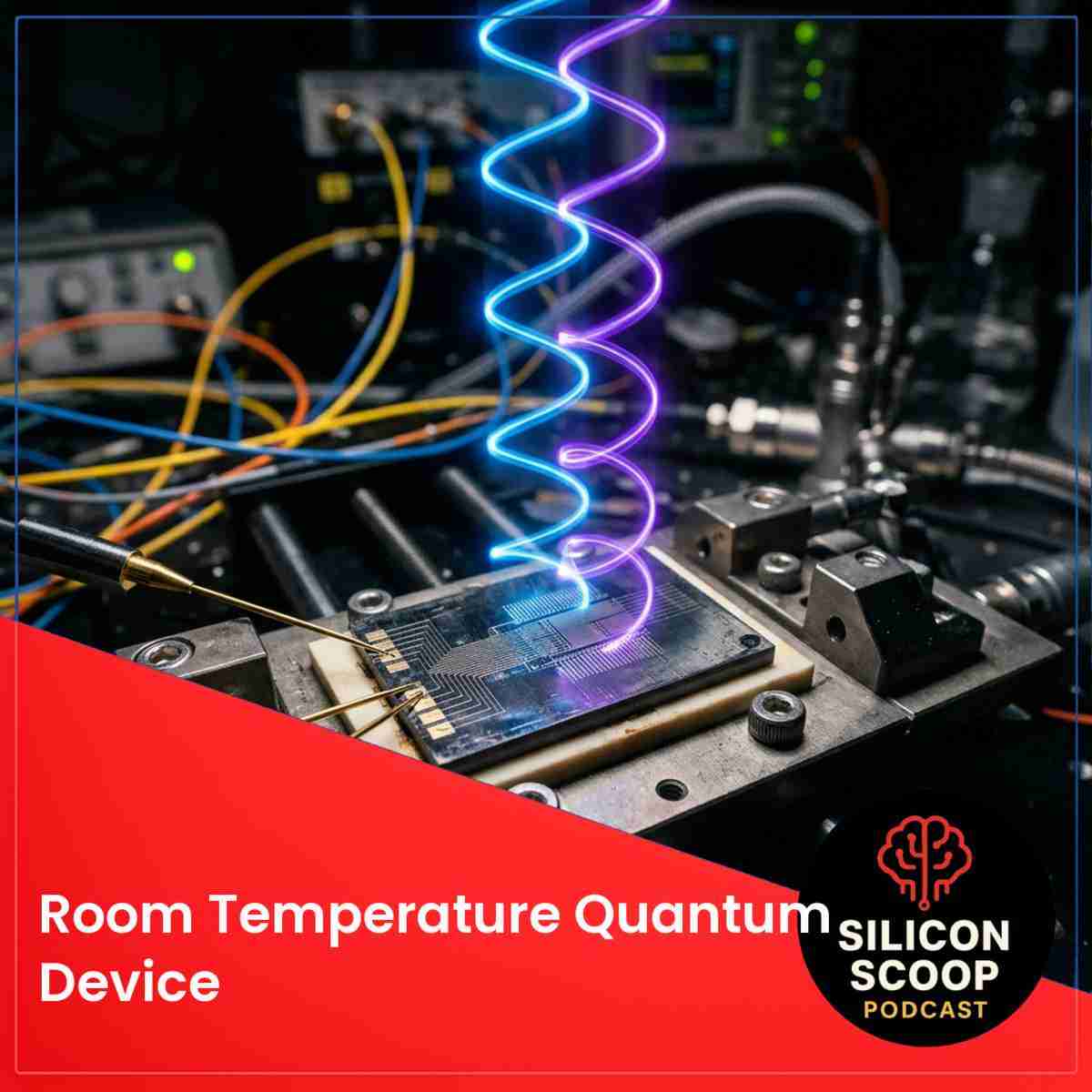
Stanford’s Room-Temperature Quantum Device Uses Twisted Light to Change Everything
Estimated reading time: 10 minutes
Key Takeaways
- A new room-temperature quantum device developed at Stanford uses twisted light to connect the quantum properties of photons and electrons — no extreme cooling required.
- It operates at room temperature (~295 K), fits on a chip roughly 3 mm × 5 mm, and targets telecom-band wavelengths around 1,550 nanometers.
- The device achieves spin-photon entanglement fidelities reported near 90% and could reshape quantum communication, secure networks, and even artificial intelligence.
Table of contents
- Stanford’s Room-Temperature Quantum Device Uses Twisted Light to Change Everything
- A Nanoscale Chip Just Made Quantum Technology Far More Accessible
- What Makes This Room-Temperature Quantum Device Different
- How Twisted Light Quantum Communication Actually Works
- The Si-MoSe2 Chiroptical Cavity: The Science Behind the Chip
- What Are Qubits and Why Does This Matter
- ⚡ Automate the Busywork You Keep Postponing
- Applications: Quantum Communication, AI, and Secure Networks
- Performance Numbers: What the Data Shows
- What Comes Next for This Research
- FAQ: 10 Common Questions About the Stanford Room-Temperature Quantum Device
A Nanoscale Chip Just Made Quantum Technology Far More Accessible
The biggest problem with quantum computers has always been simple: they need to be kept colder than outer space to work. That extreme cooling requirement makes them massive, expensive, and completely impractical for everyday use.
Stanford University researchers just changed that.
A new room-temperature quantum device developed at Stanford uses twisted light to connect the quantum properties of photons and electrons — no extreme cooling required. This breakthrough could reshape how we think about quantum communication, secure networks, and even artificial intelligence.
—
What Makes This Room-Temperature Quantum Device Different
Most quantum systems rely on temperatures near -459 degrees Fahrenheit (absolute zero) to keep their quantum states stable. The moment heat enters the picture, a process called decoherence destroys those fragile quantum states and the information stored in them.
The Stanford device sidesteps this problem entirely.
- It operates at room temperature (~295 K)
- It fits on a chip roughly 3 mm × 5 mm in size
- It achieves spin-photon entanglement fidelities reported near 90%
- It targets telecom-band wavelengths around 1,550 nanometers, making it compatible with existing fiber-optic networks
This is not a modest improvement. It is a fundamental shift in what quantum hardware can look like.
The device was described in a paper titled “Room-temperature valley-selective emission in Si–MoSe2 heterostructures enabled by high-quality-factor chiroptical cavities”, published in Nature Communications in 2025.
—
How Twisted Light Quantum Communication Actually Works
The Core Idea: Spinning Photons Transfer Spin to Electrons
At the heart of this breakthrough is a concept called twisted light quantum communication.
Normal light waves oscillate in a straight plane. Twisted light — also called chiral light — spirals like a corkscrew as it travels. This spinning motion carries a property called angular momentum, and it can be transferred to electrons.
Here is how the Stanford team made it work:
- A thin layer of molybdenum diselenide (MoSe2) sits on top of a nanopatterned silicon substrate
- The silicon nanostructures are patterned at scales roughly the size of visible light wavelengths — invisible to the naked eye
- These patterns create a chiroptical cavity that forces photons to spin in a specific direction — either up or down
- Those spinning photons then interact with electrons in the MoSe2 layer, transferring their spin
Feng Pan, postdoctoral scholar and the paper’s first author, explained it this way:
> “The Silicon nanostructures enable what we call ‘twisted light.’ The photons spin in a corkscrew fashion, but more importantly, we can use these spinning photons to impart spin on electrons that are the heart of quantum computing.”
The result is a stable spin-photon interface — a reliable quantum connection between light and matter — at room temperature.
—
The Si-MoSe2 Chiroptical Cavity: The Science Behind the Chip
Why This Material Combination Is So Powerful
The material pairing at the center of this device — a Si-MoSe2 chiroptical cavity — is what makes the room-temperature operation possible.
Molybdenum diselenide (MoSe2) belongs to a family called transition metal dichalcogenides (TMDCs). These are ultra-thin, two-dimensional materials with unique optical and quantum properties. They are especially valuable because they exhibit a quantum phenomenon called valley polarization, which is the ability to store and process quantum information in distinct energy valleys within the material.
Here is what the Si-MoSe2 heterostructure delivers:
- Optical quality (Q) factors up to approximately 450 at visible wavelengths
- A degree of circular polarization (DOP) of approximately 0.5 at room temperature
- A 13× enhancement in valley-specific radiative transition rates
- Strong chiral near-field enhancement that stabilizes valley-selective emission at room temperature
Senior author Jennifer Dionne, professor of materials science and engineering at Stanford, explained the material choice:
> “The material in question is not really new, but the way we use it is. It provides a very versatile, stable spin connection between electrons and photons that is the theoretical basis of quantum communication. Typically, however, the electrons lose their spin too quickly to be useful.”
The silicon nanophotonic cavity solves exactly that problem. By confining and enhancing the interaction between light and the MoSe2 layer, the device slows down spin loss enough to make quantum states usable.
—
What Are Qubits and Why Does This Matter
In regular computers, information is stored as bits — zeros and ones.
Qubits work differently. A qubit can be a zero, a one, or both at the same time — a quantum property called superposition. When qubits are also entangled, changes to one qubit instantly affect its partner, no matter how far apart they are.
This makes quantum systems extraordinarily powerful for:
- Encrypting and transmitting data securely
- Modeling complex molecules for drug discovery
- Solving optimization problems that would take classical computers thousands of years
- Accelerating AI inference and training
The Stanford device creates qubits from the entangled spin states of photons and electrons. The spin of a photon (up or down, based on the direction it twists) becomes entangled with the spin of an electron. This entangled pair is the basic building block of quantum information transmission.
Because the device operates at room temperature and targets telecom wavelengths, future versions could plug directly into existing fiber-optic infrastructure — meaning quantum communication networks would not require entirely new hardware.
—
—
⚡ Automate the Busywork You Keep Postponing
If your team is copying data, chasing approvals, or updating spreadsheets by hand, you’re burning time you could spend selling and delivering.
Flowgrammer builds automations that run quietly in the background so you can scale without extra headcount.
—
—
Applications: Quantum Communication, AI, and Secure Networks
Where This Technology Could Go Next
Experts in quantum photonics are careful to point out that this device is not a general-purpose quantum computer. It is a spin-photon interface — a building block for quantum communication systems.
That said, the building block matters enormously. Here is where it fits into the bigger picture:
Quantum Key Distribution (QKD) and Secure Communications
- Room-temperature, chip-integrated emitters are a key enabler for scalable quantum key distribution
- Telecom-band compatibility means this chip could slot into metropolitan fiber networks today
- Quantum-encrypted communication channels would be theoretically unbreakable
Quantum Repeaters
- Current fiber networks lose signal over long distances
- Quantum repeaters using spin-photon interfaces can extend quantum communication across continents
- This device is exactly the type of component needed inside those repeaters
AI and Edge Computing
- Market analyses identify room-temperature silicon photonic quantum components as additive to AI accelerator roadmaps
- Early commercial uses are expected in co-packaged optics, specialized sensing, and secure communication links before consumer-level applications arrive
Long-Term Vision: Quantum in a Smartphone
Pan himself acknowledged the long horizon with optimism:
> “If we can do that, maybe someday we could do quantum computing in a cell phone. But that’s a 10-plus-year plan.”
Integrating these devices into larger quantum networks will also require improvements in supporting components — light sources, modulators, detectors, and optical interconnects.
AIM Photonics
Wiley Online Library
—
Performance Numbers: What the Data Shows
The technical results behind this breakthrough are striking.
| Metric | Value |
|---|---|
| Operating temperature | ~295 K (room temperature) |
| Chip footprint | ~3 mm × 5 mm |
| Optical Q-factor | Up to ~450 |
| Degree of circular polarization | ~0.5 at room temperature |
| Valley-specific radiative rate enhancement | ~13× |
| Spin-photon entanglement fidelity | ~90% |
| Target wavelength | ~1,550 nm (telecom band) |
For context, related room-temperature nanophotonic single-photon sources in the broader research literature report Purcell factors exceeding 700 and single-photon generation rates up to roughly 3.6 × 10⁸ counts per second. These figures illustrate the performance range the Stanford platform is working toward as it matures.
The combination of high entanglement fidelity, room-temperature operation, and telecom-band wavelength compatibility places this device ahead of many competing approaches in terms of practical deployability.
—
What Comes Next for This Research
The Stanford team is not stopping here. Their next steps include:
- Exploring additional TMDC materials and new material combinations for even better quantum performance
- Investigating new quantum phenomena that may only be accessible at room temperature with this architecture
- Improving supporting technologies — including better light sources, faster modulators, and more sensitive detectors
- Moving toward integration into larger quantum network architectures
The broader quantum photonics community views TMDC monolayers combined with high-Q silicon nanophotonics as a credible route to deployable quantum repeaters and secure metropolitan networks, especially as operating wavelengths converge with telecom standards.
The chip’s silicon photonics foundation also means it could eventually be manufactured using processes compatible with existing semiconductor fabrication facilities — a critical factor for commercial scalability.
—
FAQ: 10 Common Questions About the Stanford Room-Temperature Quantum Device
1. What is a room-temperature quantum device?
A room-temperature quantum device is a piece of hardware that can create, control, and transmit quantum information without needing to be cooled to near absolute zero. Most quantum systems today require extreme cooling. This Stanford device works at normal room temperature, around 72°F (22°C).
2. What is twisted light?
Twisted light is light whose photons spiral in a corkscrew pattern as they travel. This spiral gives the photons a spinning property called angular momentum. The Stanford chip uses carefully patterned silicon nanostructures to create this twisted, or chiral, light on demand.
3. What is a qubit and how does this device make one?
A qubit is the quantum version of a computer bit. Instead of just being a zero or a one, a qubit can be both at the same time. This device creates qubits by entangling the spin state of a photon with the spin state of an electron, forming a stable quantum information pair.
4. Why does extreme cooling normally matter for quantum computers?
Quantum states are very fragile. Heat causes random vibrations that destroy quantum information through a process called decoherence. Extreme cooling reduces those vibrations enough to keep quantum states stable. This Stanford device solves the stability problem using a different approach — a specially designed cavity that keeps quantum states intact even at room temperature.
5. What is molybdenum diselenide and why was it chosen?
Molybdenum diselenide (MoSe2) is an ultra-thin, two-dimensional material from a family called transition metal dichalcogenides (TMDCs). It was chosen because it has unique quantum properties, including the ability to store quantum information in distinct energy states called valleys, and it interacts strongly with light.
6. What is a chiroptical cavity?
A chiroptical cavity is a specially shaped structure that traps and concentrates chiral (twisted) light. In this device, the silicon nanopatterns act as the chiroptical cavity. They amplify the interaction between the twisted photons and the electrons in the MoSe2 layer, stabilizing the quantum connection.
7. What is spin-photon entanglement?
Spin-photon entanglement is a quantum link between the spin state of a photon and the spin state of an electron. Once entangled, measuring one instantly tells you the state of the other. This connection is the foundation of quantum communication and quantum networking.
8. Could this technology be used in existing fiber-optic networks?
Yes, that is one of its most exciting features. The device targets a wavelength of around 1,550 nanometers, which is the standard telecom band used in fiber-optic cables worldwide. Future versions could plug into existing fiber infrastructure without requiring entirely new networks.
9. What are the most realistic near-term applications?
Experts expect the earliest uses to be in quantum key distribution for secure communications, quantum repeaters that extend the range of quantum networks, specialized sensing applications, and co-packaged optics for high-performance computing. Consumer-grade quantum devices in smartphones are at least a decade away.
10. How big is the chip and how precise is it?
The current demonstrator chip is approximately 3 mm × 5 mm — small enough to sit on your fingertip. The nanostructures etched into the silicon are about the size of visible light wavelengths, far too small to see with the naked eye. Despite this tiny scale, the device achieves spin-photon entanglement fidelities near 90%.
Sources: Nature Communications (DOI: 10.1038/s41467-025-66502-4), Stanford University, SDxCentral, MakeTechEasier, AIM Photonics, PubMed
Additional Links
Flowgrammer.ca – 💡 Unlock AI-Powered Automation! Let flowgrammer.ca handle complex workflows so you can focus on growing your business.
Flowgrammers.ca – 💡 Join Toronto’s Fastest Growing AI and Business Automation Community.
- SRED Funding Solutions – Maximize your R&D tax credits and secure funding for your innovation.
- Silicon Scoop Podcast – Stay Informed, Stay Ahead!
- Startup Talk Podcast
- Flowgrammer Youtube
- Startup Investor Drinks – Join Toronto’s Startup Community and connect with fellow startup enthusiasts and investors.
- TorontoStarts Startup and Entrepreneur Community – Become a part of Toronto’s thriving startup ecosystem.
- Workhaus – Discover flexible workspace solutions for your business needs.
- Work with The Startup Coach – Get expert guidance and mentorship for your startup journey.
- Reach out to Jon Irwin on LinkedIn – Connect with our co-host and technology expert.
Episode transcript
Read the full transcript
Craig: quantum computing has always been trapped in deep freeze labs, colder than deep space, but stanford just broke it out into the real world by twisting light like a corkscrew. they have created a nanoscaled quantum chip that runs flawlessly at room temperature. so room temperature quantum breakthrough has finally been achieved. the stanford scientists have achieved a nanoscaled chip that uses spiraling, twisted light to stably entangle photons and electrons. this allows quantum information to be transferred without the massive expensive cryogenic cooling systems traditionally required to prevent data decoherence. this bridges the gap between a fragile quantum state and existing fiber optic networks, effectively unlocking the door for unhackable citywide quantum communication infrastructure. what do you think about this, john?
Jon: yeah. i think this is really cool. so let's for those of you that don't know why quantum computers usually need extreme cooling, they use what's called superconducting qubits. and so these systems must be cooled to millikelvin temperatures. often, we're talking 10 to 20 kelvin above absolute zero because quantum information is extremely fragile. and what heat does is it causes atoms and electrons to vibrate, and that creates noise. and that noise destroys quantum states through a process called decoherence. so cryogenic cooling suppresses that noise and allows qubits to maintain their quantum properties long enough to perform calculations. and so the refrigerating infrastructure often becomes larger and more expensive than the quantum processor itself. i don't know if you've seen pictures of it, but, it's kinda cool. so let's talk about twisted light. so the stanford team created a nanoscale silicon structure that generates what physics call twisted light or light carrying orbital angular momentum. so normally, photons travel in relatively straightforward wave patterns. twisted light behaves differently. in twisted light, the photons rotate in a corkscrew like pattern as they travel through space. the twisting carries additional quantum information beyond what ordinary light can hold. so think of it this way. traditional light is like a straight arrow. twisted light is like a spinning football. and so the twist, that creates an additional degree of freedom that can be used to encode and transfer quantum information. so the key innovation here is linking photons and electrons. and so one of the biggest challenges in quantum technology is connecting light based quantum systems with matter based quantum systems. so photons are excellent for transmitting information, and electrons are excellent for storing information. right? so the stanford device creates entanglement between photon spins and electron spins. and this is important because entanglement is the foundation of quantum communication. so i think this is really cool. i love i always love, advancements in quantum. what are your thoughts on this, craig? do you have a better a better way of, describing this?
Craig: i like your football analogy, throwing a spiral versus not. just think of this update like trying to pass data across a chaotic crowded room using a smooth metal rod versus a threaded screw. normal waves of light travel flat like a smooth rod. if the room gets hot, noisy, the rod slips, vibrates, and loses its grip, destroying the data. so stanford's twisted light acts like a precision, threaded screw. as it spirals through the chip, it physical corkscrew shape locks tightly into the targeted electrons. the mechanical grip keeps the connection rock solid, even admits the buzzing thermal heat of an average room. so that's kinda my analogy. i don't know if that helps anybody, but,
Jon: no. it makes sense. and oh, go ahead. okay. the thing is this isn't really a quantum computing breakthrough. k? this is more like a quantum information breakthrough because the device itself is not a full quantum computer. it solves a critical problem of reliably transferring quantum information between light and matter without extreme cooling. that's that's what i like about this. so we've covered a lot of quantum computer computing breakthrough. we've also covered quantum information and transfer and all that sort of stuff, but this is different, and this is really cool.
Craig: this chip explicitly targets the fifteen fifty nanometer wavelength, which is the exact standard telecom bam used for global fiber optic cables today, and that's the bridge we're talking about to get from this quantum state to a normal, network. the molybdenum diselenide, i butchered those. belongs to a class of two d wonder materials. when isolated to a single layer of atoms, its physical properties fundamentally shift, transforming it from an ordinarily bulk semiconductor into a highly efficient quantum playground capable of manipulating electron spin. silicon, photonics is currently the primary battleground for semiconductor giants like intel, tsmc, and nvidia. they are aggressively pouring billions into the co packaging package optics because traditional copper wiring has hit its physical bottleneck for speed in modern ai data centers. and while the concept of light carrying orbital angular momentum, om, was mathematically proven back in 1992 by dutch physicist allen, the tech community spent decades insisting that capturing and transforming this twist inside solid state microchip at room temperature was physically impossible. so stanford just dragged quantum networking out of that cryogenic deep freeze and proved that the next generation of a hackable data security will be built on standard scalable silicon. do you think we will actually see commercial quantum chips inside everyday consumer hardware by 2036, or is this just a ten year timeline, just a venture capital hype? let us know in the comments. we'd love to hear from.
More from Silicon Scoop
All episodes
silicon-scoop · October 16, 2026
Meta’s $18 Billion Teen Safety Settlement: Soft Guardrails, Hard Leverage Over TikTok and YouTube
Deep dive on Meta teen safety settlement, social media addiction lawsuit, new Facebook Instagram time limits and pressure on TikTok YouTube age verification.
View episode

silicon-scoop · October 15, 2026
How Claude Mythos Is Reshaping Cryptanalysis: HAWK, AES and the Rise of AI-Driven Crypto Research
Claude Mythos cryptanalysis weakens HAWK post-quantum signature, speeds AES Möbius Bridge attack, and powers CryptanalysisBench benchmark in AI-driven crypto research.
View episode

silicon-scoop · October 14, 2026
Nvidia’s $12.9 Billion Hugging Face Bet: How Controlling the Open-Source Model Hub Reshapes AI Chips, Cloud, And Competition
Nvidia Hugging Face acquisition could reshape open source AI models, AI chip dominance, and the global developer model hub, raising antitrust and neutrality questions.
View episode