
Silicon Scoop · Technology
IBM Sub-1nm Chip Research Shows a Path, Not a Product
Craig Major·October 26, 2026
IBM sub-1nm chip research explained: the IBM nanostack architecture, what the lab has shown, what is projected and what still blocks production.
Estimated reading time: 10 minutes
Key Takeaways
- IBM reports nearly 100 billion transistors on a 150mm² chip, nearly twice the density of its 2nm node. The design bonds two separately made wafer structures into a 3D transistor stack.
- The 50% performance and 70% energy-efficiency figures are projections against IBM's 2nm node. IBM's lab milestones so far include dielectric bonding, dual-channel engineering and a working CMOS inverter.
- IBM plans an early design kit (PDK) for Q1 2027. It will include example standard-cell libraries and an example SRAM design, but not every model a mature commercial kit has.
- Tom's Hardware lists unresolved risks: wafer alignment, bond-interface defects, routing and power delivery, heat, extra cost and lower yields. No independent consensus on commercial viability was found.
- No funding, budget, cost or yield figures were reported in the sources. Any startup plan built on this technology rests on company targets, not production data.
Table of contents
- How IBM Nanostack Architecture Stacks Transistors Like a Two-Story Building
- What "0.7nm Chip Technology" Really Claims, and What the Lab Has Shown
- The Numbers: 100 Billion Transistors, 50% Performance, 70% Efficiency
- Why the 40% SRAM Result Is a Separate Milestone
- What Independent Sub 1nm Semiconductor Research Analysis Warns About
- IBM Doesn't Make Chips for Sale: Partners, Timelines and the Q1 2027 Design Kit
- What This Means for Startups and Small Businesses
- Frequently Asked Questions
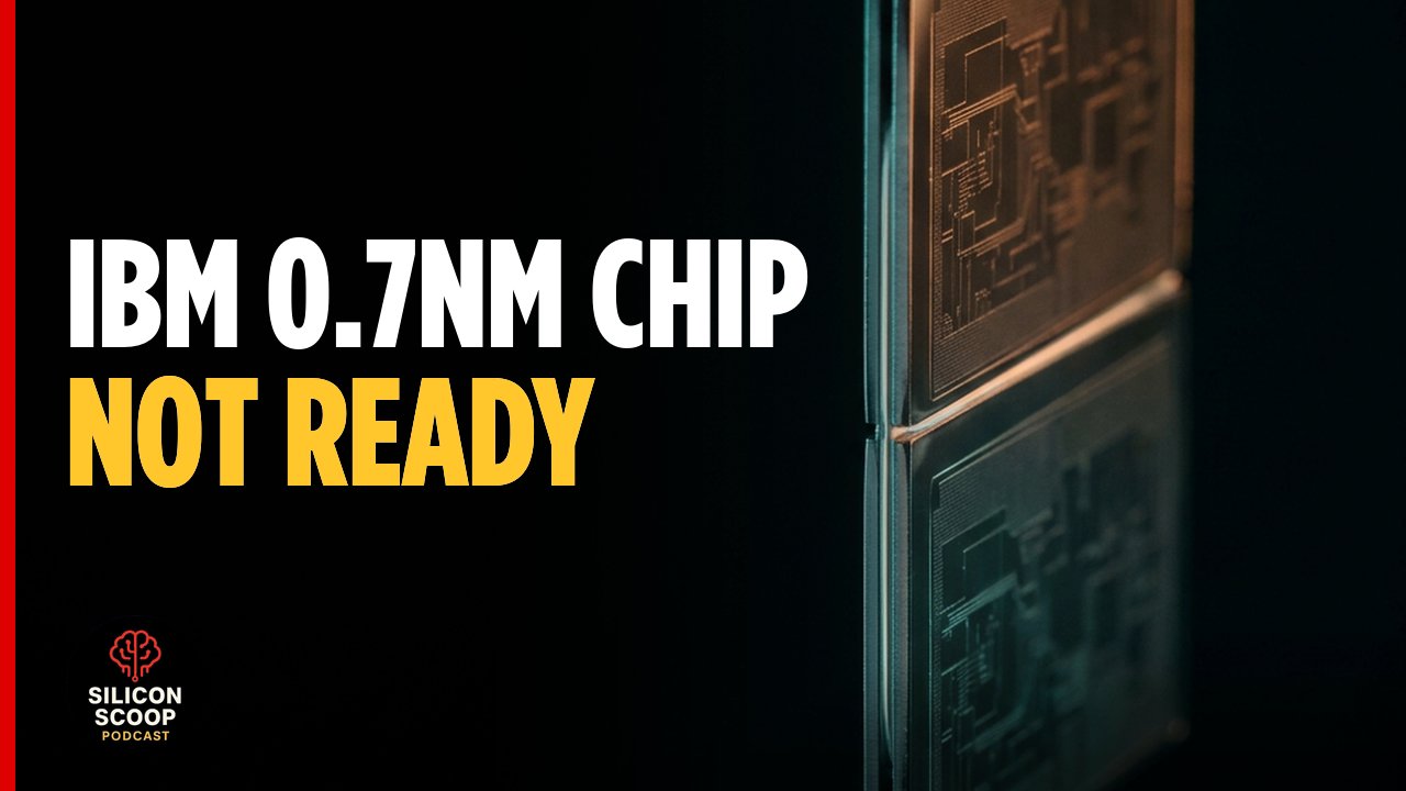
The IBM sub 1nm chip prototype packs nearly 100 billion transistors onto a 150mm² chip, almost twice the density of IBM's 2nm node. It does this by bonding two separately made wafer structures into a three-dimensional transistor stack. A wafer is the thin slice of silicon that chips are built on. IBM calls the design "nanostack" and says it was built at the 0.7nm, or 7 angstrom, node.
For chip startups and AI-hardware operators, this could eventually mean better performance per watt. But a two-wafer process with uncertain yields means high manufacturing complexity. That favors well-capitalized design and foundry partnerships. This is the post's reading of the sources, not a finding any of them states.
The title says "a path, not a product" for a reason. IBM's own production outlook is a company target, and the sources contain no cost or yield data. Below, we separate what IBM has shown in the lab from what it only projects.
Source: IBM newsroom announcement, June 25, 2026; IBM Research blog, October 13, 2026; Tom's Hardware analysis, June 26, 2026
How IBM Nanostack Architecture Stacks Transistors Like a Two-Story Building
A transistor is a tiny switch that turns current on and off. Chips hold billions of them. For years, makers have placed these switches side by side on a flat surface. That flat layout is running out of room.
IBM's answer is to build upward. According to Ars Technica's June 25, 2026 report by Jeremy Hsu, the nanostack design vertically stacks transistors in a staggered layout. That packs more of them into the same chip space.
Where nanostack came from
Nanostack builds on IBM's earlier work on nanosheet transistors. These use thin, flat sheets of silicon as the channel that carries current. That work paved the way for IBM's 2nm chip node, introduced in 2021, according to Ars Technica.
IBM first introduced the nanostack transistor architecture at the 2025 IEEE Symposium on VLSI Technology and Circuits in Kyoto, Japan. IBM cites that paper as "NanoStack Transistor Architecture for CMOS 7A Node and Beyond."
The basic building block
The basic unit is two transistors stacked and bonded together, per Ars Technica. Each transistor has three nanosheets. Each sheet is 5 nanometers thick, about 15 rows of silicon atoms. About 9 nanometers separate each sheet from the next.
Two wafers, one thin glue layer
Tom's Hardware describes the concept as using two wafer structures joined by ultra-thin dielectric bonding. A dielectric is an insulating material. The design is not a single layer of active transistors.
This matters because chips use two kinds of transistors, called n-type and p-type, that work as a pair. They are the "complementary" part of CMOS, the standard chip-making approach. Tom's Hardware's analysis says the split may let each type be tuned on its own, using different materials, process conditions, strain engineering or shapes.
The briefing describes this as an experimental architecture. It is not evidence of commercial production.
Source: Ars Technica report on IBM's 2021 2nm chip; IEEE Xplore page linked in Ars Technica's report; IBM Research blog on its 2nm nanosheet chip; Tom's Hardware analysis, June 26, 2026
What "0.7nm Chip Technology" Really Claims, and What the Lab Has Shown
IBM announced its 0.7nm chip technology on June 25, 2026. It also calls it the 7 angstrom node, because 1 nanometer equals 10 angstroms.
The name needs care. Per Ars Technica, IBM says nanostack can deliver the gains you would expect if a chip could be built with physical features smaller than 1 nanometer. The name describes expected benefits. It is not a simple ruler measurement of one part of the chip.
"World's first" is also IBM's own description. The sources retrieved for this post do not include an independent check of that claim.
The laboratory milestones
IBM's June 25 announcement says the architecture was experimentally validated through:
- CMOS integration, meaning both transistor types were built into the stack.
- Dual-channel engineering, meaning each transistor type got its own tuned channel.
- Functional CMOS inverter operation with expected switching performance.
An inverter is a basic logic gate that flips a 1 to a 0 and back. It is a small test, but a useful one. If it works, the two bonded tiers can cooperate as a circuit.
What these milestones do not prove
These are demonstrated laboratory results. They are not proof of a chip in production. The announcement's validation list names integration, channel engineering and an inverter. Treat the 100 billion transistor figure as IBM's reported density result, not as proof of a finished product.
What IBM says about it
Jay Gambetta, director of IBM Research and IBM Fellow, spoke at an advance media briefing. He said, "It's not just an incremental step, it's a meaningful leap forward." He described the technology as "pointing to a future where computing becomes significantly more powerful without a corresponding increase in energy."
That is a company leader describing company research. It is not an outside assessment.
Source: IBM newsroom announcement, June 25, 2026; IBM Research page for Jay Gambetta
Complex Systems Run Better When the Repetitive Steps Are Automated
Chip teams manage huge numbers of steps, and one slow handoff can hold up the whole line. Your business has the same kind of friction in smaller form: copying data, chasing approvals, sending the same follow-ups. Flowgrammer builds business automation that removes that manual work, saves your team hours and lets you grow without adding headcount.
The Numbers: 100 Billion Transistors, 50% Performance, 70% Efficiency
Several numbers appear in IBM's announcement. They do not all carry the same weight, so here they are sorted by evidence level.
Company-reported results
- Nearly 100 billion transistors on a fingernail-sized chip. IBM's October 13, 2026 research blog puts the chip area at 150mm².
- Nearly twice the transistor density of IBM's 2nm chip.
These are IBM-reported results from IBM's own announcements. The sources do not describe an outside lab measuring them.
Company projections
- Up to 50% higher performance at comparable power, compared with IBM's 2nm node.
- Up to 70% greater energy efficiency at comparable performance, compared with the same node.
Read the word "or" closely. The projection is one or the other, not both at once. Ars Technica describes these as projections from IBM's published technical reports. They are not measurements from shipping products.
IBM's October 13 blog repeats the same figures, along with the 40% SRAM result covered below. They are still company-reported progress and projection.
What is missing
The briefing says no financing round, project budget, commercial revenue, manufacturing cost or production yield appeared in the retrieved sources. That is a real gap. Density and efficiency numbers are exciting, but a chip only works as a business if it can be made at a price and in volume.
Founders should keep that gap in mind. A number that says "up to" is a ceiling, not an average.
Source: IBM newsroom announcement, June 25, 2026; IBM Research blog, October 13, 2026
Why the 40% SRAM Result Is a Separate Milestone
IBM also reported a 40% improvement in scaling for static random-access memory, or SRAM. IBM presented the result at the VLSI 2026 symposium. The briefing gives the paper title as "Area and Performance of Staggered-Channel Nanostack SRAM Bitcells."
SRAM is a fast kind of memory built into processors. Ars Technica notes it allows quick but energy-hungry reads and writes, which are crucial in many AI applications.
What "scaling" means here
In this context, scaling is about how much memory fits in a given area. It is a memory-density milestone. It is not a measured 40% jump in how fast or efficient a whole chip is.
This is an easy place to get confused. The 50% and 70% numbers are logic projections against the 2nm node. The 40% number is about SRAM bitcells. They should not be added together or swapped.
Why SRAM still matters
AI chips need lots of fast on-chip memory. If a stacked design shrinks that memory, designers could fit more of it, or save area for other work. That is a reasonable implication. IBM has not published a sourced chip-level result that proves it.
The sources do not give an event date for the VLSI 2026 presentation, so this post does not either.
Source: VLSI 2026 session page linked in Ars Technica's report; IBM newsroom announcement, June 25, 2026
What Independent Sub 1nm Semiconductor Research Analysis Warns About
Most coverage of this news repeats IBM's own announcement. One independent technical analysis came from Tom's Hardware, published June 26, 2026. It supports the technical interest in stacking complementary transistor tiers. It also lists problems that IBM's announcement does not quantify.
Five risks Tom's Hardware points to
- Alignment. Two advanced wafers must line up with extreme precision.
- Bond-interface defects. Flaws where the wafers meet can lower yield. Yield is the share of chips that work.
- Routing and power delivery. Getting signals and power to a 3D stack is harder than on a flat chip.
- Heat. The upper transistor tier sits farther from the heat sink.
- Cost. The analysis notes extra wafer, bonding and process-complexity costs.
None of these is a reason to dismiss the research. They are reasons to read production timelines as targets.
Is there an expert consensus?
No. The retrieved independent analysis supports the technical significance of vertical stacking. It does not establish an independent consensus that the technology is commercially viable.
No independent analyst, competitor, investor or academic reaction beyond this technical reporting was retrieved. So broader expert consensus is unavailable. Statements from IBM leaders are company views, not independent expert agreement.
The production outlook is IBM's, not a result
IBM says sub-1nm nanostack technology could reach production as early as five years after the June 2026 announcement. That is a company target. Tom's Hardware's interpretation is that this is a potential future mass-production path, not a current high-volume manufacturing result.
Source: Tom's Hardware analysis, June 26, 2026; IBM newsroom announcement, June 25, 2026
IBM Doesn't Make Chips for Sale: Partners, Timelines and the Q1 2027 Design Kit
IBM does research. According to Ars Technica, it does not manufacture commercial chips for AI data centers or consumer devices. It relies on partners to turn its designs into products.
How earlier IBM work reached the market
For its 2nm nanosheet technology, IBM partnered with Rapidus in Japan on mass manufacturing. IBM also had a partnership with Samsung in South Korea to commercialize related technology, per Ars Technica.
Ars also reports that TSMC developed nanosheet transistors on its own for its proprietary 2nm technology. It did so without direct collaboration with IBM.
For the sub-1nm node, IBM declined to name specific companies it may partner with. No manufacturing partner for nanostack has been announced in the sources.
What an IBM executive expects
Ars Technica quotes an IBM figure identified only as Bu. Bu expects commercial chips made at the sub-1nm node with nanostack could begin production as early as the next five years, and most likely within a decade.
Bu said, "It will replace nanosheet as today's mainstream in leading foundries, whether it's CPUs or GPUs." Bu added, "Within a decade, this will become another mainstream that we have invented and helped industry to transform."
These are expectations and company ambitions. They are not demonstrated production.
The early design kit
On October 13, 2026, IBM Research announced plans for an early research-and-development process design kit (PDK) for the 7-angstrom technology. A PDK is a package of rules and models that chip designers use to design for a given manufacturing process.
The status here is "planned." IBM says it intends to make the kit available in the first quarter of 2027. It is expected to include:
- Example standard-cell libraries, which are reusable building blocks of basic logic.
- An example SRAM design.
IBM said it will not initially include every model found in a mature commercial PDK.
The blog also says nanostack changes logic layout from a mostly two-dimensional arrangement to a transistor-level three-dimensional one. That brings new thermal, resistance, capacitance and device-interaction considerations for designers.
The PDK and the production outlook are different milestones. The sources do not say one is late or early compared with the other.
Source: IBM Research blog, October 13, 2026; IBM Research blog on Rapidus and 2nm production; IBM newsroom page on the IBM and Samsung announcement; TSMC 2nm technology page
What This Means for Startups and Small Businesses
You do not need a chip fab to be affected by this news. Chips set the cost and speed of AI. Here are practical steps, based on the sources.
If you build chips or AI hardware
- Treat nanostack as a research watch item. It is not a product you can buy. IBM has named no manufacturing partner.
- Mark the Q1 2027 design kit on your calendar. It is planned, not released, and it will be incomplete at first. It may help teams test ideas early, but do not expect a full commercial toolset.
- Expect partnership to matter. The two-wafer process, bonding risks and added costs suggest this will favor teams with strong capital and foundry ties. That is our inference. The sources report no cost or yield figures.
- Ask hard questions of any vendor. Ask about yield, heat handling, routing and per-wafer cost. These are the open issues independent analysis flagged.
If you run AI workloads or buy compute
- Plan around chips you can buy today. IBM's production outlook is a target of "as early as" five years, with a decade as the more likely span, per its own executive.
- Keep performance per watt in your model. IBM's goal is more computing without more energy. If it works out, power costs could matter less over time. That outcome is not proven.
- Do not quote the 50% or 70% numbers as fact. They are "up to" projections against IBM's 2nm node, and you must choose one or the other.
If you run a small business
- Do not wait for hardware to fix your slow processes. Chip progress is years out. Manual work costs you time now.
- Use hardware news as a signal, not a schedule. Real products come from teams that finish many dull steps well.
Frequently Asked Questions
Q: What is the IBM sub 1nm chip?
A: It is a research-stage chip technology IBM announced on June 25, 2026, described as built at the 0.7nm (7 angstrom) node. It uses a nanostack design that bonds stacked transistor tiers. It is not a commercial product.
Q: What is IBM nanostack architecture?
A: IBM nanostack architecture vertically stacks transistors in a staggered layout. Its basic unit is two transistors stacked and bonded together, each with three nanosheets. Tom's Hardware describes it as two wafer structures joined by ultra-thin dielectric bonding.
Q: How many transistors does the IBM sub 1nm chip hold?
A: IBM reports nearly 100 billion transistors on a 150mm² chip. That is nearly twice the density of IBM's 2nm node. IBM reported the figure itself.
Q: What does 0.7nm chip technology mean?
A: IBM calls it the 7 angstrom node, since 1 nanometer is 10 angstroms. Per Ars Technica, IBM says it delivers gains you would expect if a chip had features smaller than 1 nanometer. The name describes expected benefits, not a plain physical measurement.
Q: Is the IBM sub 1nm chip faster than current chips?
A: IBM projects up to 50% more performance, or 70% greater energy efficiency, compared with its own 2nm node. These are company projections, not measured results from shipping products. You get one gain or the other at a given setting, not both together.
Q: When will 0.7nm chips be in production?
A: IBM says production could come as early as five years after its June 2026 announcement. An IBM executive quoted by Ars Technica said it will most likely happen within a decade. This is a company outlook, not a demonstrated manufacturing result.
Q: Who will manufacture IBM's sub 1nm chips?
A: IBM declined to name partners for the newest node. IBM does not manufacture commercial chips itself. For its 2nm technology it worked with Rapidus in Japan and, on related technology, Samsung in South Korea.
Q: What are the biggest risks in sub 1nm semiconductor research like this?
A: Tom's Hardware points to wafer alignment, defects at the bond interface, harder routing and power delivery, and heat in the upper transistor tier. It also notes added wafer and bonding costs and lower yields. IBM's announcement does not quantify these.
Q: What does the 40% SRAM scaling number mean?
A: IBM presented a 40% improvement in SRAM scaling at VLSI 2026. It is a memory-density result, separate from the logic performance and efficiency projections. It is not a 40% improvement in whole-chip performance.
Q: What is IBM's planned nanostack design kit?
A: IBM plans an early research-and-development PDK for the 7-angstrom technology in the first quarter of 2027. It is expected to include example standard-cell libraries and an example SRAM design. It will not initially include every model in a mature commercial PDK.
Additional Links
Flowgrammer.ca – 💡 Unlock AI-Powered Automation! Let flowgrammer.ca handle complex workflows so you can focus on growing your business.
Flowgrammers.ca – 💡 Join Toronto's Fastest Growing AI and Business Automation Community.
- SRED Funding Solutions – Maximize your R&D tax credits and secure funding for your innovation.
- Silicon Scoop Podcast – Stay Informed, Stay Ahead!
- Startup Talk Podcast
- Flowgrammer Youtube
- Startup Investor Drinks – Join Toronto’s Startup Community and connect with fellow startup enthusiasts and investors.
- TorontoStarts Startup and Entrepreneur Community – Become a part of Toronto’s thriving startup ecosystem.
- Workhaus – Discover flexible workspace solutions for your business needs.
- Work with The Startup Coach – Get expert guidance and mentorship for your startup journey.
- Reach out to Jon Irwin on LinkedIn – Connect with our co-host and technology expert.